Electronic Manufacturing Services
Printed Circuit Board (PCB)
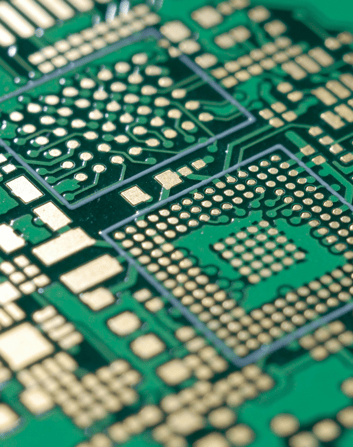
Line / Space
- Minimal Line Widtch and Space: 90µm / 90µm (3.5mil / 3.5 mil)
Vias
- Minimal Drill Hole Size: 200µm (8mil)
- PTH Hole Aspect Ratio: 1:10
- Resin Plugging: Buried & Blind Via Hole
- Via In Pad Technology: Thermal Hole Design
Product Range
- Double sided to 32 layers
- Planar Transformer PCBs
- Heavy Copper PCBs: Cu up to 10 oz
- Metal Based PCBs: Cu up to 10 oz
- Thin PCB: 0.25 mm for Double Side, 0.35 mm for 4 Layers
Surface Finishing
- Immersion Nickel/Gold (ENIG)
- Electrolytic Hard Gold
- Gold Finger Plating
- Hot-air leveled Lead Free Solder Coat
- Organic Solder Preservative (OSP)
- Carbon Contact Printing
- Plating Edge
Board Thickness
- Finish Board Thickness: 0.25 mm – 6.0 mm
Material
- Normal FR4
- Halogen Free FR4
- CEM3
- Aluminum
Flexible Printed Circuit (FPC)
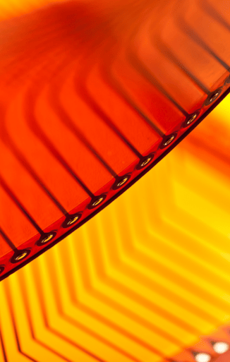
Line / Space
- Minimal Line / Space: 25 µm / 25 µm (1 mil / 1 mil)
Vias
- Mechanical Min. drill Size: 100 µm (4 mil)
- Laser Min. Drill Size: 50 µm (2 mil)
Product Thickness
- Base Material: 12.5 µm (0.5 mil) – 75 µm (3 mil)
- 2 Layers: < 80 µm
- 3 Layers: < 140 µm
- 4 Layers: < 160 µm
Stiffener
- Material: Polyimide, FR4, Aluminum, Stainless Steel
EMI
- EMI Shielding: Silver Epoxy Coating, Silver Foil Lamination
Substrate
- Base Material Type: Polyimide, PET, PEN, Liquid Crystal Polymer (LCP), Prepreg, FR4
- Adhesive Type: Acrylic, Epoxy, Prepreg
- Adhesive Thickness: 12.5 µm (0.5 mil) – 50 µm (2 mil)
- Copper Foil Type: Rolled Annealed (RA), Electro Deposited (ED), High Temperature Elongation (HTE), High Ductility (HA)
- Copper foil Thickness: 0.25 oz (9 µm) – 2 oz (70 µm)
Plating and Finishing
- Organic Surface Preservative (OSP)
- Electoless Nickel Immersion Gold (ENIG)
- Electrolytic Hard Gold
- Tin / Cu Platin
- Electrolytic Soft Gold
- Electroless Soft Nickel Gold
- Electrolytic Nickel Palladium Soft Gold
Component Mounting
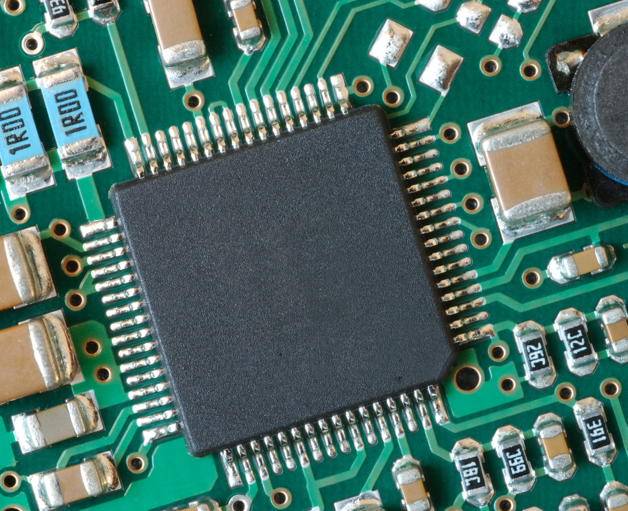
Processes
- SMT placement
- Automated through-hole-technolgy (THT) assembly of DIP, Axial and Radial components.
- Single and Double Sided processes
- SPI (solder paste inspection)
- X-Ray inspection
- AOI: Automated Optical Inspection
- Flying Probe test
- Function Test
- Conformal Coating
- Reflow soldering, wave soldering, manual soldering, induction soldering
- Polyurethane sealings and gaskets
- Polyurethane fully potting of assemblies
Membrane Switch
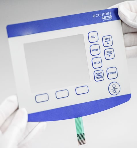
Machinery
- Screenprinting presses
- Heat and UV Tunnel ovens
- CO2 lasers
- Digital cutter
- Blanking Presses
- Embossing Presses
Capabilities
- Thickness tolerance: +/- 10%
- Dimensional tolerance: +/- 0.1mm (hard tool)
- Operating temperature range: -20°C to +50°C
- Storage temperature range:
-20°C to +80°C (no embossing)
-20°C to +50°C (Edge ad Rim soft tool embossing)
-20°C to +70°C (Hard tool embossing) - Maximum operating and storage humidity: 93%RH
- Life cycle: 1 million actuation
- Max voltage: 30V dc
Turnkey Solutions
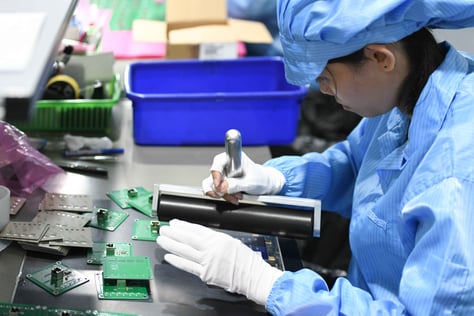
Turnkey solution is the integration of our core electronic products including PCB, FPC, PCBA, FPCA, Membrane Switch and Printed Electronic with large components and sub assemblies. When possible, we do functional tests and any other performance testing required by the customer.
Items to be incorporated include
- LCD display
- Touch screen
- Plastic molded parts
- Metal backers
- Bezel
- Light guide backlighting
- Wire harness
Printed Electronics
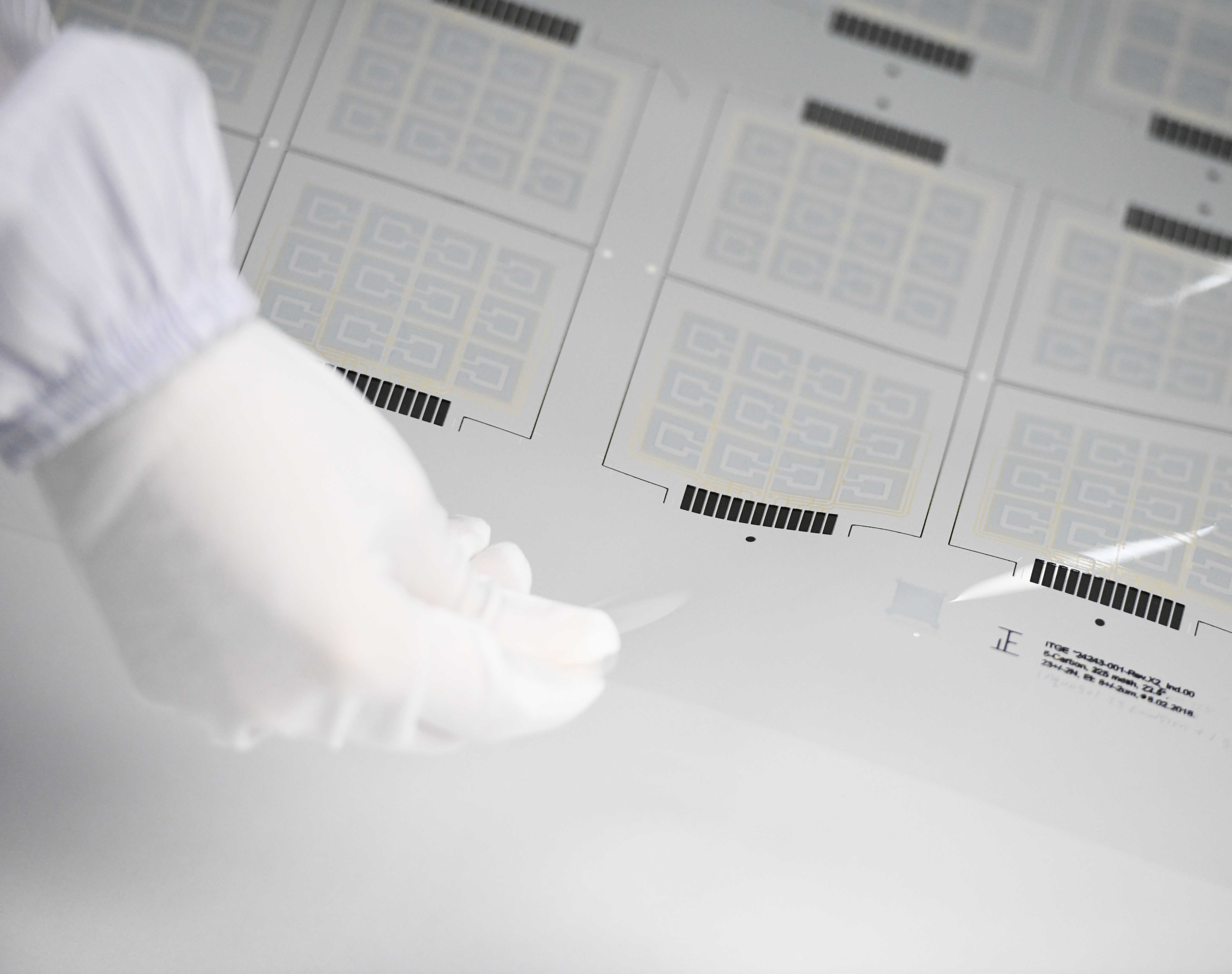
| Standard | High Level | Advanced | |
| Volume Production | Small Quantity | Sample | |
| Min Line width/spacing (μm) | 200/200 | 175/175 | 125/125 |
| Min Substrate thickness (μm) | 100 | 75 | 50 |
| Max circuit dimensions (mm) | 650 X 500 | 1200 X 800 | |
| Mechanical tolerances | +/- 0.2mm | +/- 0.1mm | +/- 0.1mm |
| Min via hole diameter | 0.2mm | 0.2mm | 0.2mm |
| Elect. Resist. tolerance | +/- 10% | +/- 8% | +/- 5% |
| Min bend radius | 1mm | 1mm | 1mm |
| Min/Max thickness | 5μm/18μm | 5μm/18μm | 5μm/18μm |
| Min component size | 402 | 402 | 402 |
| Materials | PET, PC | PI. TPU | PVC, Si, Paper |
-1.jpg?width=146&height=50&name=Kusu%20(1)-1.jpg)